Full Wave Rectifier
Full Wave Rectifier
In Full Wave Rectification, when the AC supply is applied at the input, during both the half-cycles (i.e., positive as well as negative) current flows through the load in the same direction. This can be achieved by using two crystal diodes. The two diodes conduct the current alternately.
To obtain the same direction of flow of current in the load resistors RL during positive as well as the negative half cycle of input, the two circuits are used. They are named as follows:-
- Center tapped full wave rectifier
- Full Wave Bridge Rectifier
To have detailed explanation on the two types of full wave rectifiers follow the links given above.
Center Tapped Full Wave Rectifier
The Center Tapped Full Wave Rectifier employs a transformer with the secondary winding AB tapped at the centre point C. It converts the AC input voltage into DC voltage. The two diode D1, and D2 are connected in the circuit as shown in the circuit diagram below.

Each diode uses a one-half cycle of the input AC voltage. The diode D1 utilizes the AC voltage appearing across the upper half (AC) of the secondary winding for rectification. The diode D2 uses the lower half (CB) of the secondary winding.
Operation of the Center-Tapped Full Wave Rectifier
When AC supply is switched ON the alternating voltage, Vin appears across the terminals AB of the secondary winding of the transformer. During the positive half cycle of the secondary voltage, end A becomes positive, and end B becomes negative. Thus, the diode D1 becomes forward biased, and diode D2 becomes reverse biased.
The two diodes conduct simultaneously. Therefore, when the diode D1 conducts, the diode D2 does not conduct and vice versa.
When the Diode D1 is conducting, the current (i) flows through the diode D1 load resistor RL (from M to L) and the upper half of the secondary winding as shown in the circuit diagram marked by the red color arrowheads. During the negative half-cycle, the end B becomes positive, and end A becomes negative. This makes the diode D2 forward biased, and diode D1 reverse biased.
When the diode D2 conducts while the diode D1 does not. The current (i) flows through the diode D2 load resistor RL (from M to L) and the lower half of the secondary winding as shown by the red dotted arrows.
The current flowing through the load resistor RL is in the same direction (i.e., from M to L) during both the positive as well as the negative half cycle of the input. Hence, the DC output voltage (Vout = i RL) is obtained across the load resistor.
The wave diagram of the input voltage, the current flowing through the load, and the output voltage developed across the load is shown in the figure below:

Peak Inverse Voltage of Center Tapped Full Wave Rectifier
The circuit diagram given below shows the instant when the secondary voltage attains its maximum positive value.

At this instant, Vm developed in the upper half of the secondary winding of the transformer will forward bias the diode D1. This diode conducts, and the current flows through RL, developing Vm voltage across it.
The diode D2 at this instant is reverse biased, and the voltage was coming across it is the sum of the maximum value of voltage developed by the lower half of the secondary winding and the voltage developed across the load. Hence, the peak inverse voltage across the diode D2 is 2Vm.
Advantages and Disadvantages of Center-Tapped Full Wave Rectifier
- The main advantage is that the output and efficiency are high because an AC supply delivers power during both half cycles.
The Disadvantages of the Center tapped full wave rectifier are as follows:-
- Each diode utilizes only one-half of the voltage developed in the transformer secondary, and thus the DC output obtained is small.
- It is difficult to locate the center on the secondary for the tapping.
- The diode used must be capable of bearing high peak inverse voltage. Because the peak inverse voltage coming across each diode is twice the maximum voltage across the half of the secondary winding.
Full Wave Bridge Rectifier
In Full Wave Bridge Rectifier, an ordinary transformer is used in place of a center-tapped transformer. The circuit forms a bridge connecting the four diodes D1, D2, D3, and D4. The circuit diagram of the Full Wave Bridge Rectifier is shown below.

Contents:
- Operation of Full Wave Bridge Rectifier
- Peak Inverse Voltage of Full Wave Bridge Rectifier
- Advantages of Full Wave Bridge Rectifier
- Disadvantages of Full Wave Bridge Rectifier
The AC supply which is to be rectified is applied diagonally to the opposite ends of the bridge. Whereas, the load resistor RL is connected across the remaining two diagonals of the opposite ends of the bridge.
Operation of Full Wave Bridge Rectifier
When an AC supply is switched ON, the alternating voltage Vin appears across the terminals AB of the secondary winding of the transformer which needs rectification. During the positive half cycle of the secondary voltage, end A becomes positive, and end B becomes negative as shown in the figure below.

The diodes D1 and D3 are forward biased and the diodes D2 and D4 are reversed biased. Therefore, diode D1 and D3 conduct, and diode D2 and D4 do not conduct. The current (i) flows through diode D1, load resistor RL (from M to L), diode D3, and the transformer secondary. The waveform of the full-wave bridge rectifier is shown below.

During the negative half-cycle, end A becomes negative and end B positive as shown in the figure below:

From the above diagram, it is seen that the diode D2 and D4 are under forward bias and the diodes D1 and D3 are reverse bias. Therefore, diode D2 and D4 conduct while diodes D1 and D3 do not conduct. Thus, current (i) flows through the diode D2, load resistor RL (from M to L), diode D4, and the transformer secondary.
The current flows through the load resistor RL in the same direction (M to L) during both the half cycles. Hence, a DC output voltage Vout is obtained across the load resistor.
Peak Inverse Voltage of Full Wave Bridge Rectifier
When the secondary voltage attains its maximum positive value and the terminal A is positive, and B is negative as shown in the circuit diagram below.
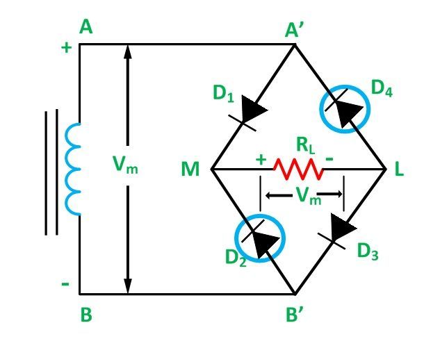
At this instant diode, D1 and D3 are forward biased and conducts current. Therefore, terminal M attains the same voltage as that A’ or A, whereas the terminal L attains the same voltage as that of B’ or B. Hence the diode D2 and D4 are reversed biased and the peak inverse voltage across both of them is Vm.
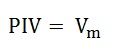
Therefore,
Advantages of Full Wave Bridge Rectifier
- The center tap transformer is eliminated.
- The output is double that of the center-tapped full-wave rectifier for the same secondary voltage.
- The peak inverse voltage across each diode is one-half of the center tap circuit of the diode.
Disadvantages of Full Wave Bridge Rectifier
- It needs four diodes.
- The circuit is not suitable when a small voltage is required to be rectified. It is because, in this case, the two diodes are connected in series and offer double voltage drop due to their internal resistance.


Comments
Post a Comment